Bench-Top MEMS Background | Supplies Needed | Formation of Microfluidic Channels | Use as Etch Mask It is possible to use photo-curable adhesives to make MEMS structures. They have lower resolution than negative photoresists such as SU8, but they do have a number of other attractive features:
Figures are from R. Delille, M. Urdaneta, S. Moseley, and E. Smela, "Benchtop polymer MEMS," J. Microelectromech. Syst., 15 (5), 1108-1120 (2006).
Figures are from R. Delille, M. Urdaneta, S. Moseley, and E. Smela, "Benchtop polymer MEMS," J. Microelectromech. Syst., 15 (5), 1108-1120 (2006).
For further information, see: R. Delille, M. Urdaneta, S. Moseley, and E. Smela, "Benchtop polymer MEMS," J. Microelectromech. Syst., 15 (5), 1108-1120 (2006). Further information and detailed instructions for fabricating various structures can be downloaded from http://ieeexplore.ieee.org/xpls/abs_all.jsp?arnumber=1707770. On the left side of the page, click “Multimedia”. The instructions below on this page are examples from that document. M. Urdaneta, R. Delille, and E. Smela, "Benchtop polymer MEMS as a low-cost educational tool," Solid State Sensors, Actuators, and Microsystems Workshop, Hilton Head, SC, Educational Poster Digest (eds. Spangler, Kenny, and Schmidt), p. 14-15 (June 4-8, 2006). Supplies Needed for Benchtop MEMS This work led to the development of MEMS education kits, for school and college students. This is possible because the photopatternable elastomer used in this technique does not require special protection equipment or chemical hoods, and does not need spinner, aligner, or other special machinery. A typical set of supplies needed for benchtop MEMS is shown here.
Formation of Microfluidic Channels, Instructions In 2000, Beebe et al. (D. J. Beebe, J. S. Moore, Q. Yu, R. H. Liu, M. L. Kraft, B.-H. Jo, and C. Devadoss, "Microfluidic tectonics: A comprehensive construction platform for microfluidic systems," PNAS, 97 (25), 13488–13493 (2000).) demonstrated a method to fabricate a complete microfluidic channel system based on liquid-phase photopolymerization and lithography of hydgrogels, which they called microfluidic tectonics (micro-FT). In-situ creation of the channels is attractive because the structures are fabricated all at once without the need for later alignment and bonding. Such structures can also be made using these commercially available adhesives. The following instructions were originally prepared by S. Moseley and M. Urdaneta. For further information, refer to R. Delille, M. Urdaneta, S. Moseley, and E. Smela, "Benchtop polymer MEMS," J. Microelectromech. Syst., 15 (5), 1108-1120 (2006). For detailed instructions on fabricating various other structures, download the supplementary materials (pdf).
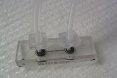
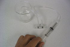
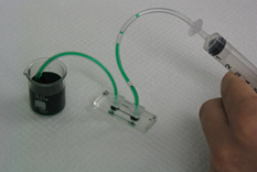
Connect commercially available nylon fittings (such as 1/16” McMaster Carr 5117k41) and hoses (Tygon Super-Soft High Purity Tubing, McMaster Carr 9449k11, OD 3/16 in, ID 1/16 in, wall 1/16 in) via the holes drilled in the substrate. Place one hose in beaker of acetone and connect the other hoses to a syringe (e.g. 10 ml disposable). Create suction with the syringe and draw acetone through the channel. This clears the undeveloped 3108 out of the channel.
To avoid the use of plastic wrap to prevent the photopatternable elastomer from sticking to other surfaces, since plastic wrap can create “wiggles” of nonuniform height on the surface, Sylgard 184 polydimethylsiloxane (PDMS) base precursor (Dow Corning) can be wiped onto any solid surface to leave a thin coating. The Loctite 3108 will not stick to this treated surface. This can be done to e.g. the mask, allowing it to be brought into direct contact with the photopatternable elastomer and then pealed off after exposure. Instructions for Using 3108 as an Etch Mask These instructions were originally prepared by S. Moseley and Mario Urdaneta.
Background | Supplies Needed | Formation of Microfluidic Channels | Use as Etch Mask
|
|
|
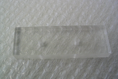
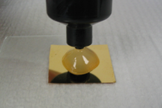
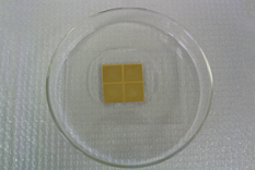
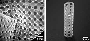 Examples of free-standing, flexible
structures made using Loctite 3108 are shown here.
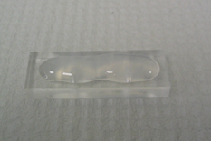
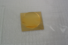
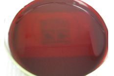
Examples of free-standing, flexible
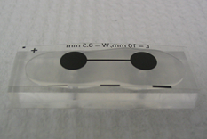
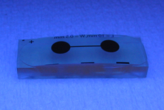
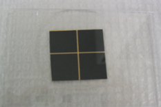
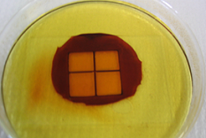
structures made using Loctite 3108 are shown here.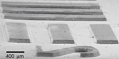 An example of the features you can obtain in Loctite 3340 by
photolithography are shown here.
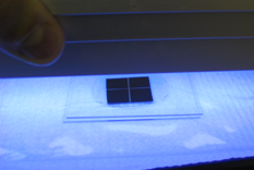
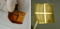
An example of the features you can obtain in Loctite 3340 by
photolithography are shown here.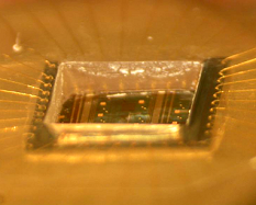 One can also use the 3340 for short-term packaging (a week or two) of CMOS chips for immersion in cell medium, as discussed in the
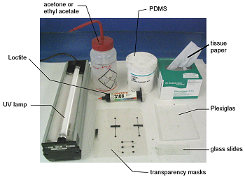
©2013