Conjugated Polymer Actuators
Modeling Bilayer Behavior Modeling Inplane Strain | Modeling the Bending of Trilayers With Benjamin Shapiro, we have been working to understand actuator bending. Timoshenko’s model for bilayer bending due to differences in coefficients of thermal expansion [S. Timoshenko, "Analysis of bi-metal thermostats," J. Opt. Soc. Am., 11, 233-256 (1925)] provides a good starting point for an analysis of actuator bending. For constant moduli and CTEs, the curvature where the
It should be noted that there is an optimum thickness ratio, given E1 and E2. When plotting the curvature versus the thickness ratio m, there is a peak that arises from trading off a higher force due to adding electroactive material and making bending harder by making the beam thicker. This will be true regardless of the two materials, and actuator designers should bear this optimum in mind. For PPy(DBS)/Au bilayers, the optimum thickness ratio was ~5:1, and this changes only slightly with total bilayer thickness. At this ratio, a radius of curvature of only 2 µm was achieved with an Au layer of 500 Å.
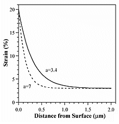
The actuation strain of PPy is, unfortunately, not constant throughout the thickness of the material (z-direction), which is especially notable in thin films. In the bulk, the inplane strain is ~3%. By examining the bending of a large number of bilayer microactuators with different m = h1/h2, and modeling the bending by taking into account the possibility of a strain gradient in the PPy film, we found that the strain at the electrolyte/PPy interface is ~17%, and that it decreases to 3% over a distance of ~1 µm. The figure on the left illustrates the dependence of strain with distance from the electrolyte surface for two different model parameters. Modeling the Bending of Trilayers Large interfacial stresses at the polymer/electrode interface caused by repeated expansion and contraction of the polymer during actuation sooner or later result in adhesive failure. Delamination can be improved by roughening the polymer/electrode interface, as shown here link to Preventing Delamination section. Another approach to preventing delamination is to use a “buffer layer” between the polymer and the electrode. By optimizing the thickness and modulus of this layer, the stress at that interface can be reduced to zero, with no loss of curvature and only a small loss in force. For PPy(DBS) 450 nm thick on Au, this ideal intermediate layer should be 150 nm thick and have a modulus of 5 GPa.
For further information see:
|
|
|
 It should also be noted that the actuation strain
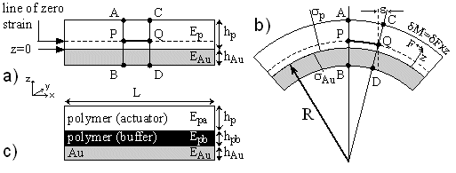
©2013