Cell-Based Sensing
Microsystem Components Sensors | Lidded Vials | Au Plating | Packaging Sensors Abshire’s group has developed a suite of sensors for monitoring cells cultured on the chip surface in various ways. We fabricate MEMS structures over these, and do the packaging. Contact Imager
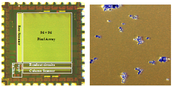
H. Ji, P. A. Abshire, M. Urdaneta, and E. Smela, "A CMOS contact imager for monitoring cultured cells," IEEE Int. Symp. Circuits and Systems (ISCAS05), Kobe, Japan, p. 3491 - 3494 (23-26 May, 2005). H. Ji, D. Sander, A. Haas, and P. Abshire, "A CMOS contact imager for locating individual cells," IEEE Int. Symp. Circuits and Systems (ISCAS06), Kos, Greece, p. (submitted abstract) (May 21-24, 2006). Fluorescence Sensor
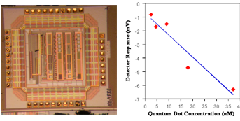
For further information, see: H. Ji, M. Dandin, E. Smela, and P. Abshire, "Integrated fluorescence sensing for lab-on-a-chip devices," IEEE/NLM Life Science Systems & Applications Workshop, Bethesda, MD (July 13-14, 2006). S. B. Prakash, N. M. Nelson, A. M. Haas, V. Jeng, P. Abshire, M. Urdaneta, and E. Smela, "Biolabs-on-a-chip: monitoring cells using CMOS biosensors," Proc. IEEE/NLM Life Science Systems & Applications Workshop, Bethesda, MD (July 13-14, 2006). M. Dandin, P. Abshire, and E. Smela, "Optical filtering technologies for integrated fluorescence sensors," Lab Chip, 7 (8), 955-977 (2007). H. Ji, D. Sander, M. Dandin, E. Smela, and P. Abshire, "Integrated fluorescence sensor for UV-excitable fluorescent probes," IEEE Transactions on Circuits and Systems I (in preparation) (2007). D. Sander, M. Dandin, H. Ji, N. Nelson, and P. A. Abshire, "Low-noise CMOS fluorescence sensor," International Symposium on Circuits and Systems 2007 (ISCAS07), New Orleans, LA, USA, p. accepted for publication (May 27-30, 2007). Capacitance Sensor
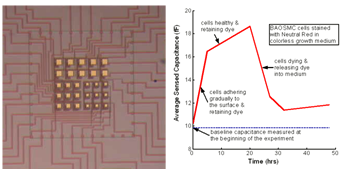
For further information, see: S. B. Prakash, P. Abshire, M. Urdaneta, and E. Smela, "A CMOS capacitance sensor for cell adhesion characterization," Int. Symp. Circuits & Systems (ISCAS05), Kobe, Japan, (IEEE), vol. 4, p. 3495 - 3498 (23-26 May, 2005). S. B. Prakash and P. A. Abshire, "A CMOS capacitance sensor that monitors cell viability," Proc. IEEE Sensors Conference, Irvine, CA, p. 1177-1180 (Oct. 31-Nov. 3, 2005). S. B. Prakash and P. A. Abshire, "On-chip capacitance sensing for cell monitoring applications," IEEE Sensors J., 7 (3), 440-447 (2007). Bioamplifier
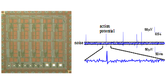
For further information, see: Potentiostat
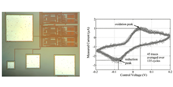
For further information, see: S. B. Prakash, P. Abshire, M. Urdaneta, M. Christophersen, and E. Smela, "A CMOS potentiostat for control of integrated MEMS actuators," Int. Symp. Circuits & Systems (ISCAS06), Kos, Greece (May 21-24, 2006). S. B. Prakash, M. Urdaneta, M. Christophersen, E. Smela, and P. Abshire, "In situ electrochemical control of electroactive polymer films on a CMOS chip," Sens. Act. B, 129 (2), 699-704 (2008).
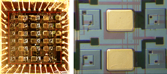
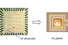
The CMOS chips arrive from the manufacturer with aluminum electrodes. Since Al is not biocompatible, it is covered with Au by electroless plating. The techniques we use were developed by Mario Urdaneta.
For further information, see: R. Delille, M. Urdaneta, S. Moseley, and E. Smela, "Benchtop polymer MEMS," J. Microelectromech. Syst., 15 (5), 1108-1120 (2006).
|
|
|
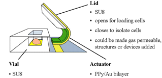
 Methods for fabricating lidded vials on the tiny CMOS chips were developed by
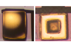
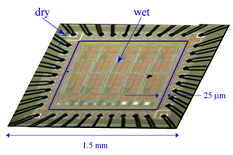 The challenges of packaging these chips are 1) the small distance between the bond pads, which must remain dry, and the chip surface, which must be exposed to the cells and the cell medium and 2) the bond wires rising by more than 100 mm above the chip surface.
 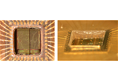 We are currently using Loctite 3440, a photopatternable adhesive, which can last for a couple of weeks in an incubator before failure. The figure shows overhead and oblique views. We are pursuing other packaging methods to improve the lifetime.
 ©2013